
POWER
SEMICONDUCTOR
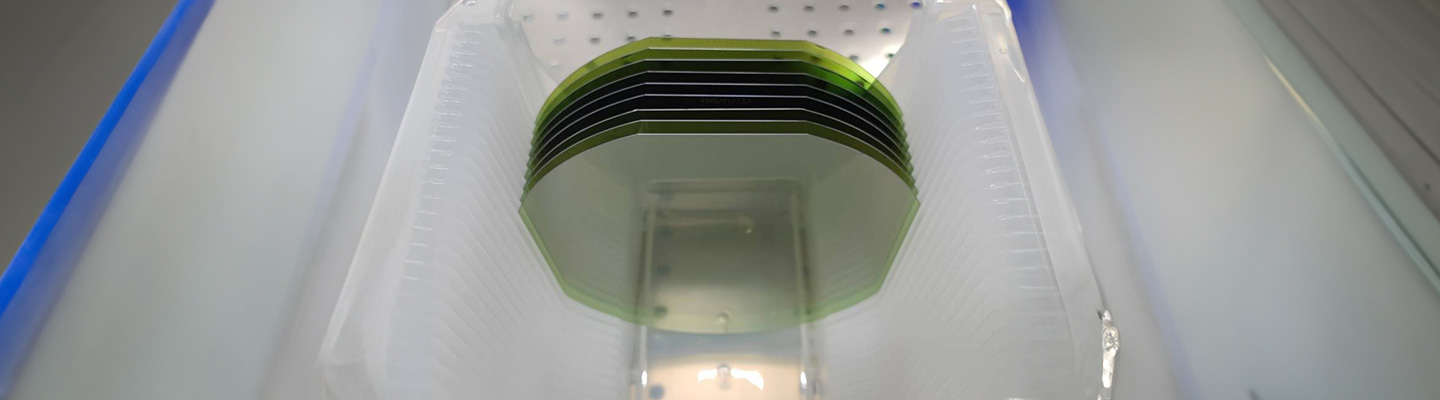
SiC
A “Power Semiconductor” is a semiconductor that literally controls power, characterized for “Conducting” electricity easily and working “insulator” to prevent the flow of electricity.
Basically, Power Semiconductors can be divided into 3 functions ; Amplification, Rectification, and Switching. Mostly used in Power Conversion (Changing Voltages, Frequencies), Changing DC ↔ AC, charging & suppling power grids with less power loss, providing a stable electricity source to various home appliances and electrical equipment.
Recently, Power Semiconductors are expending their application to various fields such as Electric Vehicles, Solar Power Generation, and demand is expected to increase rapidly due to the increased demand of the Industry of 4th Revolution (IT, Smart EV, Autonomous Vehicles, Robots, Solar, IoT, Smart Grid, Aerospace, 5G Communication)
In particular, the application of Power Semiconductors is expected to expand further as the importance of Energy Saving due to the Climate Crisis, so that the 3rd Generation Semiconductors, which is Compound Semiconductor (SiC, GaN) demand will be more increased.
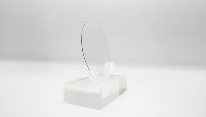
SiC Epi Wafer
Epi Wafer (n-Type : 8” & 6”)

| Item | 8 inch | 6 inch |
|---|---|---|
| Diameter | 200.0mm ± 0.5mm | 150.0mm ± 0.25mm |
| Flat / Notch | Notch | Flat Zone Length 47.5 mm±2.5 mm |
| Thickness | 500 μm ± 25μm | 350 μm ± 25μm |
| Crystal Orientation | (4± 0.5)° off-axis toward <11-20> | (4± 0.5)° off-axis toward <11-20> |
| Resistivity | 0.015 ~ 0.028 Ω·cm | 0.015 ~ 0.025 Ω·cm |
| MPD | ≤0.5cm-2 | ≤0.2cm-2 |
| Buffer Layer Thickness | 1μm | 1μm |
| Buffer Layer Concentration | 1.00E+18 | 1.00E+18 |
| Epi Layer Concentration | * 7.5E15 ~ 1.1E16 | * 8E15~1.1E16 |
| Epi Layer Thickness | * 5um ~ 16um | * 5um ~ 16um |
| Test Pattern | 25 pionts,X cross | 17 pionts,X cross |
| KDDY (2mm X 2mm) | ≥ 95% | ≥ 95% |
| TTV | ≤ 20μm | ≤ 15μm |
| WARP | ≤ 70μm | ≤ 50μm |
| Bow | ± 60μm | ± 40μm |
* Red Color : Can be Customizing
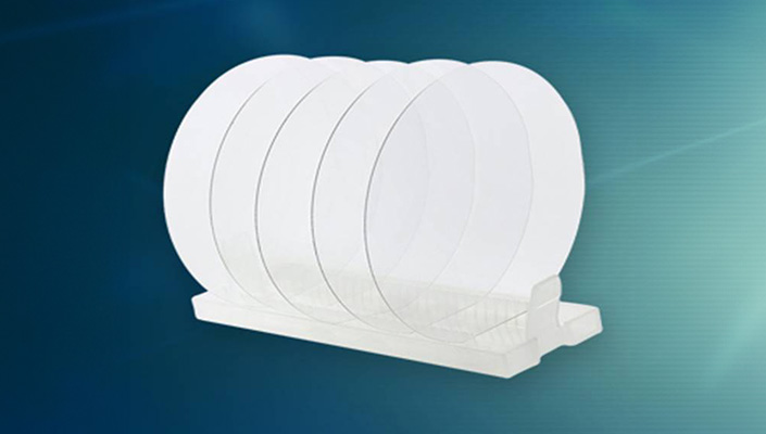
SiC Substrate
n-Type Substrate (8” & 6”)
| Item | 8 inch | 6 inch |
|---|---|---|
| Diameter | 200.0mm ± 0.5mm | 150.0mm ± 0.25mm |
| Flat / Notch | Notch | Flat Zone Length 47.5 mm±2.5 mm |
| Thickness | 500 μm ± 25μm | 350 μm ± 25μm |
| Crystal Orientation | (4± 0.5)° off-axis toward <11-20> | (4± 0.5)° off-axis toward <11-20> |
| Surface condition | Polished | Polished |
| Resistivity | 0.015 ~ 0.028 Ω·cm | 0.015 ~ 0.025 Ω·cm |
| MPD | ≤0.2cm-2 | ≤0.2cm-2 |
| BPD | ≤ 1500 | ≤ 1500 |
| TSD | ≤ 200 | ≤ 200 |
| TTV | ≤ 15μm | ≤ 10μm |
| WARP | ≤ 50μm | ≤ 40μm |
| BOW | ± 30μm | ± 25μm |
Semi-Insulated Substrate (6” & 4”)
| Item | 6 inch | 4 inch |
|---|---|---|
| Diameter | 150.0mm ± 0.2mm | 99.8 ~ 100.0mm |
| Thickness | 500 μm ± 25μm | 500 μm ± 15μm |
| Surface Orientation | <0001> ± 0.2° | <0001> ± 0.2° |
| FWHM (0004) | ≤ 80 arcsec | ≤ 50 arcsec |
| Resistivity | ≥ 1E9 Ω·cm | ≥ 1E10 Ω·cm |
| Primary Flat Orientation | {10 10} ± 1.0° | {10 10} ± 5.0° |
| Primary Flat / Notch | Notch 1.0 ~ 1.5mm | Flat Zone Length 32.5 mm±1.5 mm |
| MPD | ≤ 0.15cm-2 | ≤0.3cm-2 |
| TTV | ≤ 5μm | ≤ 7μm |
| WARP | ≤ 25μm | ≤ 25μm |
| BOW | ± 15μm | ± 15μm |
- Address
- 305, B, 33, Gwacheon-daero 7-gil, Gwacheon-si, Gyeonggi-do, Republic of Korea
- CEO
- H. J. Jun
- TEL
- +82-70-4521-8194
- inform@jtnu.co.kr
COPYRIGHT © 2023 JTNU ALL RIGHTS RESERVED.
Privacy Policy