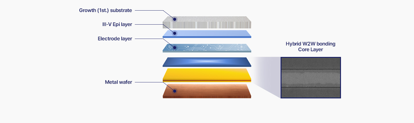
Hybrid W2W bonding technology
Our Hybrid wafer-to-wafer bonding technology using metal substrates is a proven technique not only in terms of characteristics, but also in yield and mass productivity.
Technology Consulting Program
In the case of special technologies such as Hybrid wafer bonding, we are actively participating in the equipment required for technical consulting and making efforts to ensure complete technology transfer.
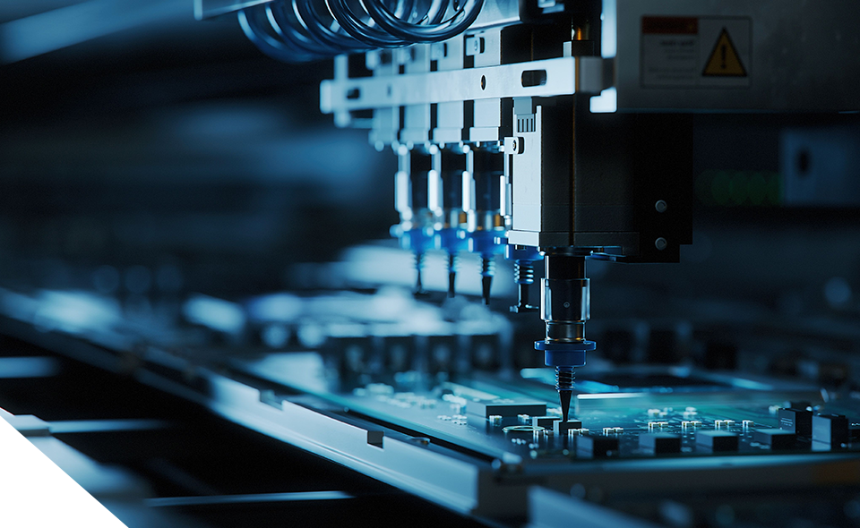
Vertical LED process using Metal substrate
Advanced LED
· High-Power LED for Automotive, Lighting, etc.
· Micro LED
Unit process technology
· Hybrid W2W bonding technology : Core layer tech.
Wafer bonding & Laser lift-off tech. (include equipment design)
Laser scribing tech. (include equipment design)
| Materials | Thermal conductivity (W/mK) |
Coeff. of thermal expansion (10-6/K) |
Remark |
|---|---|---|---|
| GaN | 130 | 5.6 | III-V raw materials |
| GaAs | 46 | 6.8 | III-V raw materials |
| Al2O3 Sapphire | 42 | 7.5 | 1st. Substrate, Bad heat sink capability |
| Si | 150 | 3.7 | Cheaper, but need to be thinning |
| SiC | 270 | 4.2 | Very expensive |
| CuW (10% Cu) | 188 | 6.4 | High tech. required on Wafer bonding, (Laser) Scribing, Lift-off processing |
| MoCu | 163 | 6.9 | |
| Mo | 139 | 5.5 |
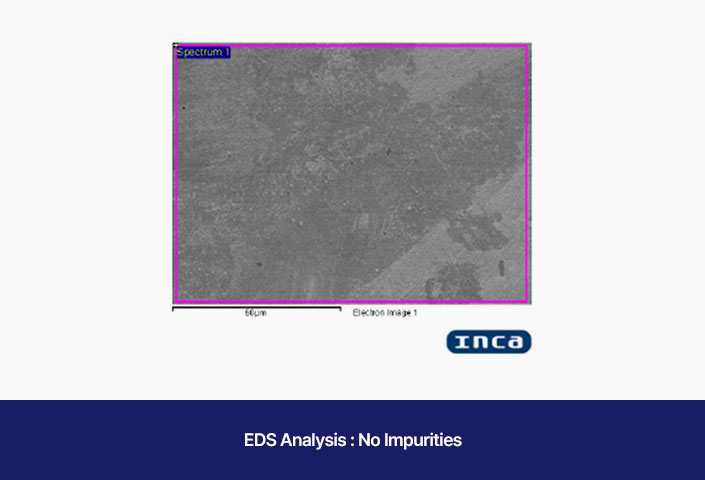
Wafer Bonding Materials
Metal substrate
| Item | Range |
|---|---|
| Size | 6 inch, 4 inch, 2 inch |
| Thickness (㎛) | 50 ~ 200 ± 10 |
| Flatness (㎛) | 100 ~ 250 |
| Coeff. Of Thermal Expansion (10-6/K) | 5.5 ~ 7.2 |
| Thermal Conductivity (W/mK) | 139 ~ 203 |
| Heat Capacity (J/kgK) | 170 ~ 280 |
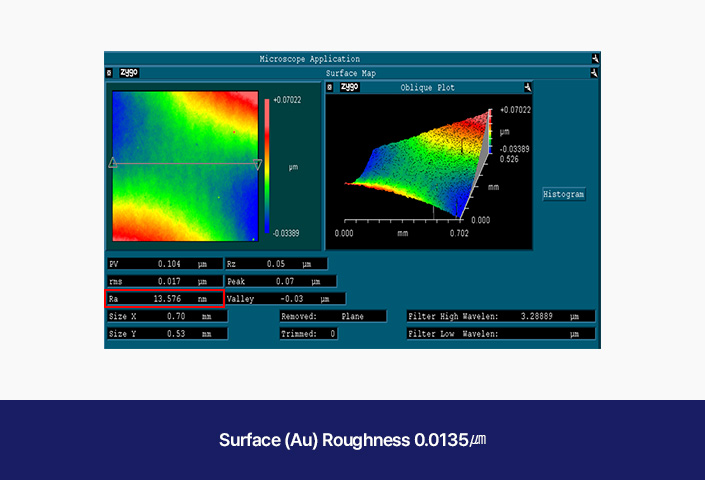
Surface treatment
| Description | |
|---|---|
| Surface | Mirror Like (鏡面), Foggy (霧面) |
| Surface Roughness | Ra 0.01 ㎛ ~ |
| Plating Material | Cu, Cr, Ni, Sn, Au, Ag, Zn (Alloy available) |
| Plating Thickness | 0.001㎛ ~ 3000㎛ |
- Address
- 305, B, 33, Gwacheon-daero 7-gil, Gwacheon-si, Gyeonggi-do, Republic of Korea
- CEO
- H. J. Jun
- TEL
- +82-70-4521-8194
- inform@jtnu.co.kr
COPYRIGHT © 2023 JTNU ALL RIGHTS RESERVED.
Privacy Policy